
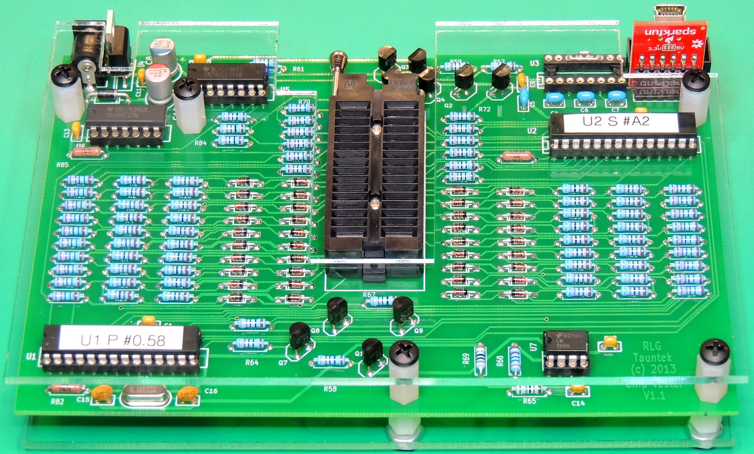
I just finished a popular kit project used for testing 7400 series, and some 4000 series logic IC’s. It was recently featured in CuriousMarc’s YouTube channel titled “Viewer-designed, Tauntek TTL IC tester!”.
I have been planning on building my own logic IC tester for several years, but have been putting it off for many reasons. I decided to purchase this kit for two reasons. Either it would completely fit my needs, so that I would not need to design and build my own. Or it would give me additional ideas or inspiration to build my own. (or both)
The kit cost me $43.40 USD including shipping, and included an unpopulated PC board and two programmed PIC microcontroller chips.
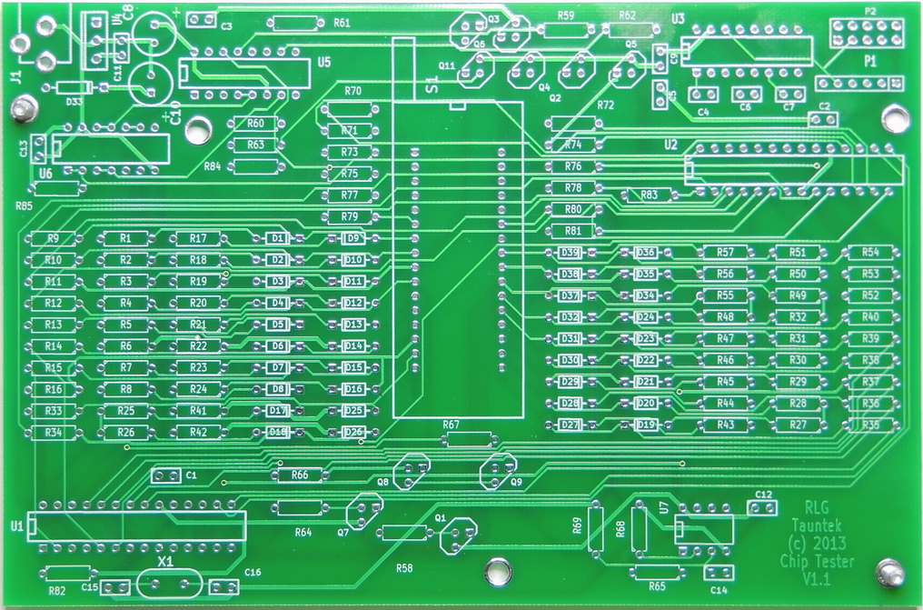

Parts to populate the board from DigiKey cost $65.00 USD not including taxes or shipping. It took me a full afternoon and evening to assemble and test the kit, which also included testing all transistors, diodes, resistors, and capacitors before soldering then on the board. There were a total of 162 individual components to solder to the board, and I used some Kester 44 rosin-core 0.020″ solder which worked well with a Hakko T15-BLL fine point conical tip soldering iron.
I did find one design issue while building the board with the operational amplifier U7B. The inputs and output of the 2nd unused op-amp were left floating with no connections. This is something that many people overlook, and is not recommended practice. a great explanation why not to do this can be found in a Texas Instruments TechNotes publication sboa204a.

The fix was fairly easy using a pair of 12K ohm 1/10th watt resistors and a jumper. This forms a voltage divider between ground and +5 volts resulting of a voltage of approximately 2.5 volts tied to pin 5 of U7 the + input. The output pin 7 is tied to the — input pin 6 with a jumper.

I also made some other small changes to the design by changing the values of the 5 volt regulator capacitors. The board layout had an odd lead spacing of 3.00 mm, while most radial capacitors have a standard spacing of either 2.5 or 3.5 mm. I ended up using some Conductive Polymer Aluminum Solid Capacitors that I had in stock. I lowered the input capacitor C10 to 33 uF at 20volts and raised the value of the output capacitor C8 to 150 uF at 10 volts.
I also changed capacitors C4 thru C7 on the RS-232 level shifter U3 from 0.1 uF to a ceramic 1 uF at 50V X7R capacitor. This is the recommended value in the recent Texas Instruments specification sheet for the MAX232.


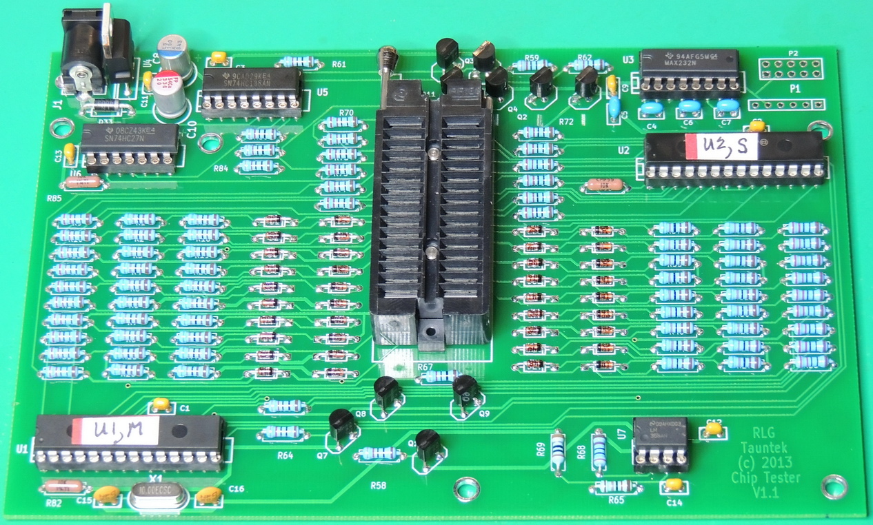
One last modification before I can use the board. The P2 connector is setup for connecting a RS-232 serial connection using a 2X5 10 pin IDC to a DB9 IDC connector. This was probably useful 10 years ago when this was originally designed, but not as useful today with the lack of 9 pin serial ports on most computers. The designer did include a 6 pin header P1 for connecting a USB to Serial adaptor. The designer states that this “Maybe the correct pinout” but is untested.

It is not the correct pinout for a TTL serial to USB adaptor. So a small adjustment is needed to make it compatible. As designed the circuit routes RS-232 output levels, which are +/- 10 volts to pin 5 of header P1, and looks for the same input levels from pin 4. I used a Sparkfun FTDI Basic TTL serial to USB adaptor which requires 0 — 5 volt TTL levels in its inputs and outputs. The simple fix for this is to remove the RS-232 level shifter IC U3, and add two jumpers. This routes the RX and TX TTL signals from microprocessor U1 to pins 4 and 5 of header P1. Pin 1 of header P1 is ground.
I used several trimmed leads from installed capacitors to make the jumpers. Jumper 1 connects pin 11 to 14 on socket U3, and jumper 2 connects pin 12 to 13 on the same empty socket.
I tried several serial terminal programs at baud rates up to 19.2K which is the listed maximum speed with good results. Best results are obtained using a VT100 mode emulation as this is the format that the board outputs.


Testing a 74AHC125 CMOS 3‑state output quad bus buffer logic IC.
When disabled the outputs are turned off presenting a high-impedance to the bus as can be seen in row 3 of the test as floating outputs (F).

Overall it is a good logic IC tester kit, but needs a few tweaks to make it excellent. The firmware works well with no issues that I noticed. I was fairly unimpressed with the trace sizes of the 5 volt and ground busses on the board. There was plenty of room on the board to increase the trace sizes, and add separate current paths for the device under test (DUT), microprocessors, pull-ups, and RS-232 level shifter. There were adequate bypass capacitors installed on most active devices though, which is always good to see.
Only the first 19 pins on the DUT are tied to A to D converters for analogue voltage monitoring on individual pins. For most common logic IC’s this is good enough, as there are very few logic IC’s with over 20 pins.
It is not open source software or hardware which is fine, but may have benefited from the community by going that route. The developer is actively updating the library of logic IC’s that it can test. To update the library the primary microprocessor must be reprogrammed with an updated hex file.
I have also been looking at the Retro Chip Tester Professional by 8Bit-Museum.de , and may build my own version of a logic IC tester later this year if my budget permits.
Spoiler below,

Thanks for the re-engineering hints, especially the serial interface and the floating op-amp pins.
When do you expect to release your own tester?
Hi Jack,


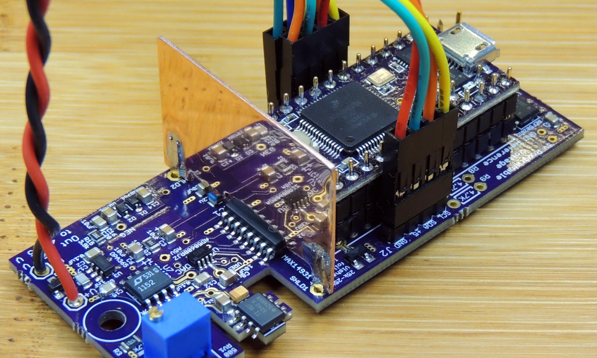
A working revision of the hardware is complete (0.14), and a low-level testing program has been installed for the ADC’s on the SPI bus, and the I/O Expander on the I2C bus.
Reading all 28 A to D converter input channels in less than 1 millisecond with 16 sample averaging per channel.
Screen capture of ADC readings with Pullup and Pulldown resistors enabled on all channels. Pin 14 is selected as ground, and pin 21 set as 5 volt VCC.
I currently have another board revision ready with mosfets and other changes, but am low on funds with the holidays so it may be a while before it is ordered.
The software will likely take the most time, as I am much better with the hardware side of projects. So may release it next Fall.
Thanks, Happy Holidays
Greg (Barbouri)