
After finishing the IceTube clock version 1.31 build for myself, I was ready to work on the board design for some IceTube clocks as gifts. I could have used the existing V 1.31 boards, but I wanted to use an up to date design that incorporated all the hardware improvements over the past 10 years while still staying with a thru-hole design.
This updated design is based on jarchie’s (John Archie) xmas-icetube clock revision D board. He had incorporated most of the hardware features that I wanted for my new batch of clocks, along with a vastly improved firmware update.
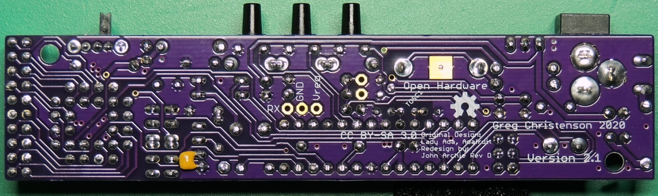
One of the most important hardware improvements for me was the ability to properly drive the IV-18 tube to specifications (providing more even display illumination and preventing cathode poisoning). Some other features of the design are the inclusion of an one wire temperature sensor near the oscillator crystal to provide highly accurate temperature compensation of the crystal frequency, reset pull-up resistor, micro-controller power decoupling capacitor, GPS connection pads, along with an improved board layout while still maintaining physical compatibility with Ver. 1.X board switches and connectors.
While there are so many things that I really liked about jarchie’s Rev D board, there were also a few areas that I thought needed some improvement.
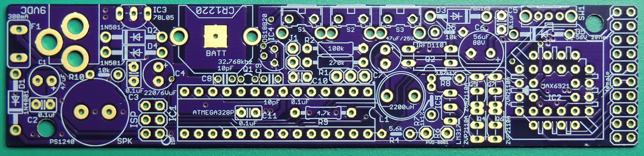
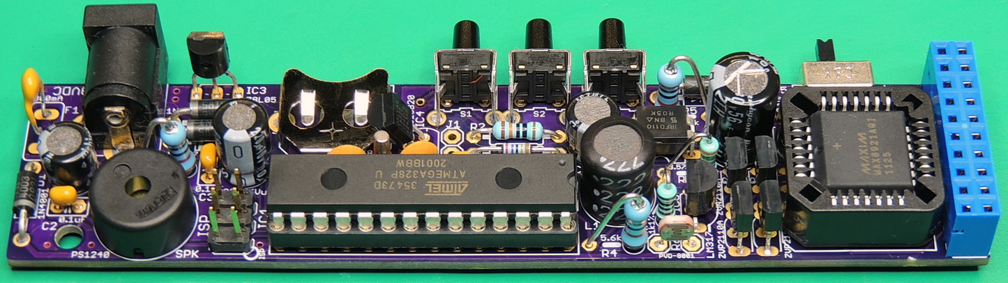
The first area I worked on was increasing the size of all power traces, with special attention to the micro-controller, high-voltage, and filament sections. I then worked on increasing signal conductor width and improving spacing between conductors and pads. With a few small moves of components, conductors, and added ground via’s, I was able to significantly improve the existing ground pour on both top and bottom planes. Next I added component values and adjusted font sizes to fit the available space. The side board also benefited from trace width and spacing adjustments, along with a small increase in height to accommodate the needed changes.
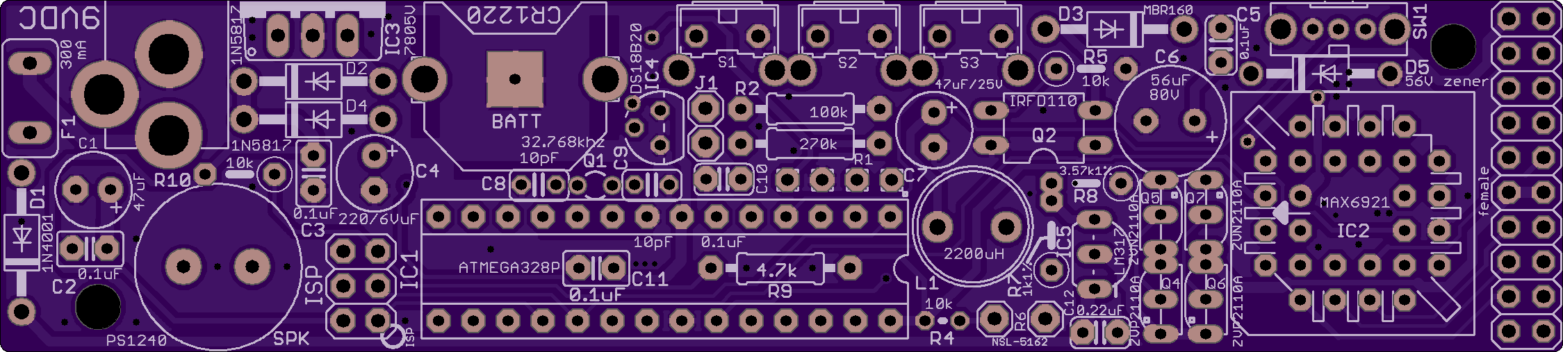
After receiving my version 2.1 boards from OSH Park and adding the components, I checked that my modification didn’t break anything. All was well, but I was seeing some oscillations on IC5 which is the LM317 voltage regulator for the filament drive circuit.
I ended up adding a 0.22 uF 50 volt ceramic capacitor on the back side of the board directly from the LM317’s input to the ground pin of the photo-resistor R6, which corrected the issue.
That prompted version 2.2 of the main board which added C12 the LM317 decoupling capacitor, changing the footprint of IC3 to the TO-220 vertical version, reducing the footprint size of R4 which is part of the photo-resistor circuit, reducing the pad size and adding a TX pad to the GPS pads, along with some other minor improvements.
When I get the updated V2.2 boards, my plan is to try a TO-220 style 5 volt switching regulator similar to the one I used on the V 1.31 build. The current V 2.1 boards draws 110 mA at 9 volts, while the V 1.31 board draws 59 mA at 9 volts which is a significant energy savings. Part of the extra current draw other than the linear regulator is the filament drive circuitry operating at the proper voltage and current.
The firmware that jarchie produced is very robust and works extremely well. It supports both the Adafruit version 1.X boards and the advanced hardware Rev D / 2.X boards.
Settings for the type of board and options are set in a very well documented config.h file and are easy to modify before compiling the firmware. The config.h file is well worth a full read thru to understand what options are available. I ended up defining the filament as 3.3 volts instead of the default 5 volts as my specific IV-18 tubes had an extremely bright filament glow at night when running at the default 5 volts, and a just noticeable glow when operating at 3.3 volts. This can vary between IV-18 tubes, and was possibly enhanced by the lower voltage drop due to the increased trace width and lower resistance on the AC1 and AC2 board traces.

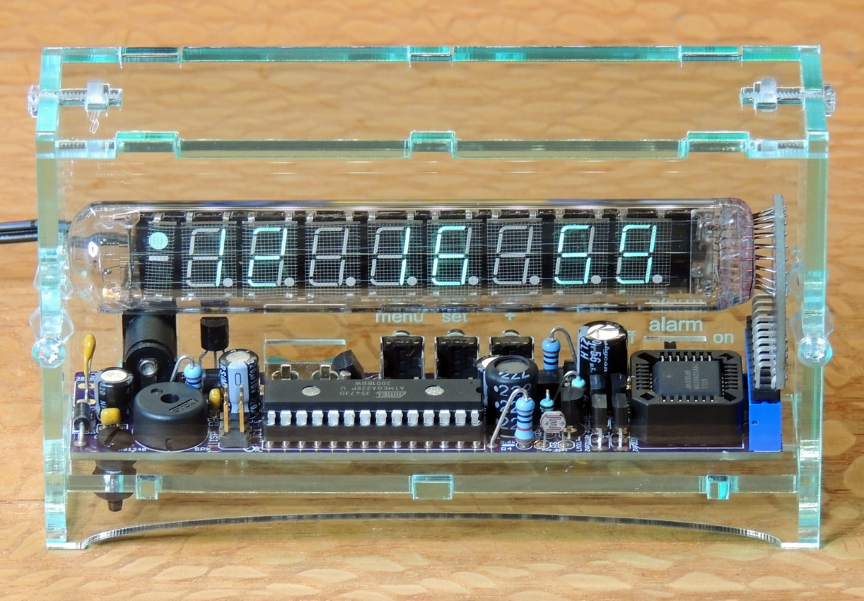
The enclosure was laser cut using 1/8″ (3mm) green edged glass tinted Acrylic, which gives it a slightly green color when looking at the edge of the acrylic but is mostly clear when looking thru the sheets. I also used some clear polycarbonate screws and nuts to hold the pieces together which were purchased from McMaster-Carr.
Original documentation with updated EagleCAD 7.7 schematic and board files for version 2.2 main and side pcb’s IceTubeClockV22.zip
OSH-Park shared projects Main PCB Rev. 2.2
OSH-Park shared projects Side PCB Rev. 2.2
John Archie’s GitHub original documentation
Great write-up! I built this according to your schematic and it worked perfectly. The only minor issue I ran into is that C6: 80v 56uf cap isn’t correct in the BOM. The cap listed in the BOM is 33uF 100v. Minor issue but thought I’d pass the info along.
Hi Sean,
Congratulations, good to hear that your project was a success! If you get a chance, post a picture on Twitter @breviceps @oshpark
I was able to find a Rubycon electrolytic capacitor with a higher capacitance rating at a slightly lower max voltage rating.
The 33 uF @ 100V capacitor works fine, but the additional 22 uF of the 56uF unit provides additional ripple reduction.
The reduced voltage rating should not be a problem, as the circuit is limited to around 56 volts by Zener diode D5.
The Rubycon 56 uF capacitor part number is 80ZLH56MEFC8X11.5 and has a 8000 Hrs @ 105°C rating.
Greg (Barbouri)
Thank you for the superb work you have done to improve the Ice Tube Clock and its PCBs. Also for sharing your interesting projects in such detail !
Please could you add a link to your Rev 2.2 Gerber files if possible, or perhaps email the files to me? I would really like to build the Rev 2.2 version of the clock. The OSH-Park links have stopped working.
OSH-Park links have been repaired.
Thank you for restoring the links
Hi, I just mounted my tube clock by your design, great v22 update, thanks.
Just one note so far that I found out, on the PCB mask the C1 and C2 are swapped.
Also R4 on your design is a 10K but BOM says is a 5.6K, I installed the 5.6K since I ordered all parts from the BOM list, should I changed it for the 10K?
Because of this my C6 is a 33uF, is it important to be a 56uF instead as you replied before to another comment here?
Just to finalize… the J1 jumper is really for what, since it disables the R2 and C10?
I can’t find any documentation about it.
Thanks again for all this.
For C1 and C2, they are in parallel between the same two points. It should not make any difference which goes where.
The jumper disables (pulls to ground) the battery sensor. You would need to look at the firmware to see what the processor does with that input.
I am in process of building one of these and will be looking at the firmware code in the next few weeks.